

Pin Diagram and Pin description of 8237
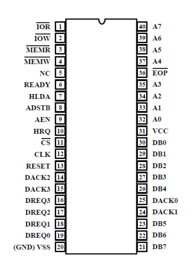
VCC
POWER: a5V supply.
VSS
GROUND: Ground.
CLK Input
CLOCK INPUT:Clock Input controls the internal operations of the 8237A and its rate of data transfers. The input may be driven at up to 5 MHz for the 8237A-5.
CS Input
CHIP SELECT:Chip Select is an active low input used to select the 8237A as an I/O device during the Idle cycle. This allows CPU communication on the data bus.
RESET Input
RESET: Reset is an active high input which clears the Command, Status, Request and Temporary registers. It also clears the first/ last flip/flop and sets the Mask register. Following a Reset the device is in the Idle cycle.
READY Input
READY: Ready is an input used to extend the memory read and write pulses from the 8237A to accommodate slow memories or I/O peripheral devices. Ready must not make transitions during its specified setup/hold time.
HLDA Input
HOLD ACKNOWLEDGE: The active high Hold Acknowledge from the CPU indicates that it has relinquished control of the system busses.
DREQ0 ±DREQ3 Input
DMA REQUEST: The DMA Request lines are individual asynchronous channel request inputs used by peripheral circuits to obtain DMA service. In fixed Priority, DREQ0 has the highest priority and DREQ3 has the lowest priority. A request is generated by activating the DREQ line of a channel. DACK will acknowledge the recognition of DREQ signal. Polarity of DREQ is programmable. Reset initializes these lines to active high. DREQ must be maintained until the corresponding DACK goes active.
DB0 ±DB7
DATA BUS: The Data Bus lines are bidirectional three-state signals connected to the system data bus. The outputs are enabled in the Program condition during the I/O Read to output the contents of an Address register, a Status register, the Temporary register or a Word Count register to the CPU. The outputs are disabled and the inputs are read during an I/O Write cycle when the CPU is programming the 8237A control registers. During DMA cycles the most significant 8 bits of the address are output onto the data bus to be strobed into an external latch by ADSTB. In memory-to-memory operations, data from the memory comes into the 8237A on the data bus during the read-from-memory transfer. In the write-to-memory transfer, the data bus outputs place the data into the new memory location.
IOR Input/Output
I/O READ: I/O Read is a bidirectional active low three-state line. In the Idle cycle, it is an input control signal used by the CPU to read the control registers. In the Active cycle, it is an output control signal used by the 8237A to access data from a peripheral during a DMA Write transfer.
IOW Input/Output
I/O WRITE: I/O Write is a bidirectional active low three-state line. In the Idle cycle, it is an input control signal used by the CPU to load information into the 8237A. In the Active cycle, it is an output control signal used by the 8237A to load data to the peripheral during a DMA Read transfer.
EOP Input/Output
END OF PROCESS: End of Process is an active low bidirectional signal. Information concerning the completion of DMA services is available at the bidirectional EOP pin. The 8237A allows an external signal to terminate an active DMA service. This is accomplished by pulling the EOP input low with an external EOP signal. The 8237A also generates a pulse when the terminal count (TC) for any channel is reached. This generates an EOP signal which is output through the EOP line. The reception of EOP, either internal or external, will cause the 8237A to terminate the service, reset the request, and, if Autoinitialize is enabled, to write the base registers to the current registers of that channel. The mask bit and TC bit in the status word will be set for the currently active channel by EOP unless the channel is programmed for Autoinitialize. In that case, the mask bit remains unchanged. During memory-to-memory transfers, EOP will be output when the TC for channel 1 occurs. EOP should be tied high with a pull-up resistor if it is not used to prevent erroneous end of process inputs.
A0 ±A3 Input/Output
ADDRESS: The four least significant address lines are bidirectional three-state signals. In the Idle cycle they are inputs and are used by the CPU to address the register to be loaded or read. In the Active cycle they are outputs and provide the lower 4 bits of the output address.
A4 ±A7 Output
ADDRESS: The four most significant address lines are three-state outputs and provide 4 bits of address. These lines are enabled only during the DMA service.
HRQ Output
HOLD REQUEST: This is the Hold Request to the CPU and is used to request control of the system bus. If the corresponding mask bit is clear, the presence of any valid DREQ causes 8237A to issue the HRQ.
DACK0 ±DACK3 Output
DMA ACKNOWLEDGE: DMA Acknowledge is used to notify the individual peripherals when one has been granted a DMA cycle. The sense of these lines is programmable. Reset initializes them to active low.
AEN Output
ADDRESS ENABLE:Address Enable enables the 8-bit latch containing the upper 8 address bits onto the system address bus. AEN can also be used to disable other system bus drivers during DMA transfers. AEN is active HIGH.
ADSTB Output
ADDRESS STROBE: The active high, Address Strobe is used to strobe the upper address byte into an external latch.
MEMR Output
MEMORY READ: The Memory Read signal is an active low three-state output used to access data from the selected memory location during a DMA Read or a memory-to-memory transfer.
MEMW Output
MEMORY WRITE: The Memory Write is an active low three-state output used to write data to the selected memory location during a DMA Write or a memory-to-memory transfer.
PIN5 Input
PIN5: This pin should always be at a logic HIGH level. An internal pull-up resistor will establish a logic high when the pin is left floating. It is recommended however, that PIN5 be connected to VCC