

Pin Diagram and Pin description of 8085
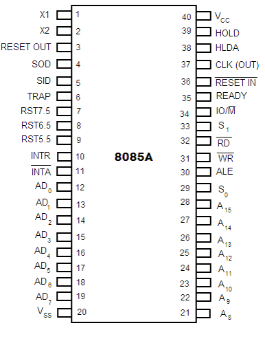
8085 is a 40 pin IC, The signals from the pins can be grouped as follows
1. Power supply and Clock frequency signals:
Vcc: + 5 volt power supplyVss: GroundX1, X2 : Crystal or R/C network or LC network connections to set the frequency of internal clock generator.
The frequency is internally divided by two. Since the basic operating timing frequency is 3 MHz, a 6 MHz crystal is connected externally.
CLK (output)-Clock Output is used as the system clock for peripheral and devices interfaced with the microprocessor.
2. Address Bus:
A8 - A15: (output; 3-state)It carries the most significant 8 bits of the memory address or the 8 bits of the I/O address.
3. Data bus:
AD0 - AD7 (input/output; 3-state)- These multiplexed set of lines used to carry the lower order 8 bit address as well as data bus.
- During the opcode fetch operation, in the first clock cycle, the lines deliver the lower order address A0 - A7.
- In the subsequent IO / memory, read / write clock cycle the lines are used as data bus.
- The CPU may read or write out data through these lines.
4. Control and Status signals:
ALE (output) - Address Latch Enable.- It is an output signal used to give information of AD0-AD7 contents.
- It is a positive going pulse generated when a new operation is started by uP.
- When pulse goes high it indicates that AD0-AD7 are address.
- When it is low it indicates that the contents are data.
RD (output 3-state, active low)
- Read memory or IO device.
- This indicates that the selected memory location or I/O device is to be read and that the data bus is ready for accepting data from the memory or I/O device
WR (output 3-state, active low)
IO/M (output) - Select memory or an IO device.- This status signal indicates that the read / write operation relates to whether the memory or I/O device.
- It goes high to indicate an I/O operation.
- It goes low for memory operations.
5. Status Signals:
S1:
S2:
It is used to know the type of current operation of the microprocessor.
| IO/M | S1 | S0 | OPERATION |
|---|---|---|---|
| 0 | 1 | 1 | Opcode fetch |
| 0 | 1 | 0 | Memory read |
| 0 | 0 | 1 | Memory write |
| 1 | 1 | 0 | I/O read |
| 1 | 0 | 1 | I/O write |
| 1 | 1 | 0 | Interrupt acknowledge |
| Z | 0 | 1 | Halt |
| Z | x | x | Hold |
| Z | x | x | Reset |
6. Interrupts and Externally initiated operations:
TRAPRST 7.5RST 6.5RST 5.5INTAReset In (input, active low)Reset Out (Output)7. Direct Memory Access (DMA): Tri state devices:
HOLD signal is generated by the DMA controller circuit. On receipt of this signal, the microprocessor acknowledges the request by sending out HLDA signal and leaves out the control of the buses. After the HLDA signal the DMA controller starts the direct transfer of data.READY (input)READY signal after completing the present job to access the data.8. Single Bit Serial I/O ports:
SID (input) Serial input data lineSOD (output) Serial output data lineThese signals are used for serial communication.